Built for UH Mānoa’s Astronomy & Physics Department's High Energy Physics Group, this custom PCB interfaces an Arduino Mega 2560 with up to four QPADL-3 delay lines, enabling precise 10-picosecond adjustments for RF testing. The PCB was designed in Kicad.
ToC
1. Introduction
Designing and assembling the programmable delay line daughter board was a milestone in my journey into PCB design. As my first project in this domain, it presented an opportunity to learn how to use KiCad for PCB layout and to explore part libraries like SnapEDA, Ultra Librarian, and Octopart for sourcing components. Although the board is relatively simple, its creation involved integrating the Arduino Mega 2560 with Gigabaudics QPADL-3 programmable delay lines and preparing it for use within a larger system controlled by an RFSoC ZCU111.
2. Manufacturing
2.1. Components
- Arduino Mega 2560 (Quantity: 1)
- Gigabaudics QPADL3 (Quantity: 4)
- Custom daughterboard(files in Google Drive)
- DB25 IDC Board Male Header
Digikey Part Number A33167-ND (Quantity: 4)
(https://www.digikey.com/en/products/detail/te-connectivity-amp-connectors/5103308-6/1114905)
- 36-Pin Header
Digikey Part Number SSW-118-03-G-D-ND (Quantity: 1)
(https://www.digikey.com/en/products/detail/samtec-inc/SSW-118-03-G-D/7880952)
- DB25 IDC Cables
- DB25 IDC Cable Board Female Header
Digikey Part Number AKC26H-ND (Quantity: 4)
(https://www.digikey.com/en/products/detail/te-connectivity-amp-connectors/1658621-6/825404)
- DB25 IDC Cable Female Connector
Digikey Part Number 1000570035 (At least 4 ft of cable)
(https://www.digikey.com/en/products/detail/molex-temp-flex/1000570035/4368625)
- DB25 IDC Cable Ribbon
Digikey Part Number 2057-DB25-SF-M1-ND (Quantity: 4) (https://www.digikey.com/en/products/detail/samtec-inc/SSW-118-03-G-D/7880952)
- 6-20 V (Recommended 7-12 V) DC Power Source (Quantity: 1)
- USB-A/USB-C to USB-B Cable (Quantity: 1)
2.2. Schematic and Wiring Diagram

Figure 1. The wiring diagram and schematic for the Arduino Mega 2560, QPADL3, and daughter board.
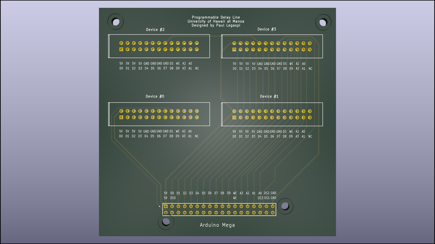
2.3. Daughter Board for Programmable Delay Lines

Figure 2. A render of the top layer of the programmable delay line daughter board.


2.4. Relevant Data Sheets and Manuals
Arduino Mega 2560:
https://content.arduino.cc/assets/Pinout-Mega2560rev3_latest.pdf
Gigabaudics QPADL3:
http://www.gigabaudics.com/QPADL3/QPADL3.pdf
2.5. Assembling the Programmable Delay Line Daughter Board and IDC Cables
The PCB for the programmable delay line daughter board was manufactured by PCBWay. All remaining parts for the daughter board were purchased from Digikey.
- Solder Digikey Parts SSW-118-03-G-D-ND (36-pin header) and A33167-ND (DB25 IDC Board Male Header) to the corresponding labeled areas of the daughter board. Although not mandatory, it is recommended that the side of the DB25 IDC Board Male Header with only one indentation be facing towards the 36-pin header. This follows the standard convention for IDC cables and will hopefully lead to less confusion when creating the DB25 cables that will be connected to the board.
Note: The first prototype does not adhere to standard convention and should not be used as a reference if intending to follow the standard convention.
- Refer to the following video guide for guidance on creating DB25 IDC ribbon cables: https://www.youtube.com/watch?v=40oXq8tCrBA&t=10s&pp=ygUPZGIyNSBpZGMgY2FibGVz.
Note: Regardless of whether you decided to follow standard convention when creating the DB25 IDC ribbon cables, make sure that one end of the ribbon cable is directly aligned and touching the side of the DB25 IDC Board Male Header that is connected to the 5V and D0 pins of the DB25 IDC Board Male Header. After confirming that this is the case, insert the other end of the ribbon cable through the side of the DB25 IDC Female Connector with 13 pins.
- To avoid shorting the programmable delay lines, check that the cables are creating the correct connections between the Arduino and the QPADL-3’s, insert a wire into each pin of the DB25 IDC Cable Female Connector and insert the other end of the cable into the programmable delay lines. Use a multimeter to probe the pins on 1) the Arduino Mega 2560 or any unused DB25 IDC Board Male Header on the daughter board and 2) the wire attached to the DB25 IDC Cable Female Connector to verify connections.
2.6. Setting Up the Arduino Mega 2560 and Programmable Delay Line Board
- Attach the programmable delay line daughter board to the Arduino Mega 2560 via its 36-pin header.
- If the Arduino Mega 2560 is not already configured with the correct program files, download pdl.ino from Google Drive using the following link: https://drive.google.com/drive/folders/1UtiLncrf5sNqrBZj8K6weRVO-dFhUMpl?usp=drive_link. Upload the program to the Arduino using the Arduino IDE. No additional libraries are required to interface with the programmable delay lines.
- Attach the desired number of QPADL-3 programmable delay lines to the board with DB25 IDC ribbon cables.
- Insert the 6-20 V power supply into the DC barrel-jack connector of the Arduino Mega 2560. Although it is possible to power all 4 programmable delay lines with the power provided to the Arduino Mega 2560 with USB, it is recommended to use a dedicated external power supply to ensure that the Arduino is able to supply enough current to all 4 programmable delay lines.
Note: The programmable delay lines can draw supply currents ranging from 50 mA to 250 mA. It will, however, only draw 200 mA for high programming rates. If the configured delay is not changed rapidly or is set to a static amount, the QPADL-3 current draw will be close to 50 mA. If this is the case, powering the Arduino through USB may suffice but is still not recommended if using all 4 programmable delay lines.
2.7. Programmable Delay Line (Gigabaudics QPADL-3)
The Arduino Mega 2560 and its accompanying daughter board are designed to work with the Gigabaudics QPADL-3. The QPADL-3 is a 4-channel programmable delay line that can be configured to set a delay of up to 10,230 picoseconds based on a provided number of steps. A DB25 connector is used to power and program the QPADL-3. The relevant pin-out diagram is shown in Figure 4. Pins 1–10 (D0–D9) correspond to the 10 bits used to specify the delay as a number of steps, with each step being 10 picoseconds.

2.8. Design Process for the Programmable Delay Line Daughter Board

The current design of the daughter board for the programmable delay line extends the design created by Ben Rotter from controlling 2 programmable delay lines to 4 programmable delay lines. Figure 7 shows a picture of Rotter’s prototype.
The first step in the design process was to determine the functionality of the previous existing prototype and test its functionality. The code used for Rotter’s prototype and instructions for interacting with the prototype could not be found. To address this issue, a multimeter was used to determine the pins used by the Arduino to communicate commands to the programmable delay line. The results of this process were used to create code compatible with the previous prototype and verify its functionality with the QPADL-3.
2.8.1 Design Software
MITS EASY CAD was used for initial attempts to design a daughter board that can interface with 4 programmable delay lines. The software offers all of the necessary functionality to create a working design but is limited in its ability to easily modify designs. The design process was transitioned to Kicad to more easily modify designs for the PCB.
The design was created directly in Kicad’s PCB Editor without first creating a schematic in the Schematic Editor. Although this is valid, it is recommended to create the schematic first before transitioning to designing the layout for the PCB. Net classes, labels, and wires describing the connections between components are more easily configured in the Schematic Editor and are transferred to the PCB Editor. Following this workflow will help accelerate the design process by minimizing the need to manually select tracks and pads in the PCB Editor and designate a corresponding net class for each individual connection.
The design process for creating the daughter board also involved using components that are not available as symbols or footprints in Kicad. Although it is possible to create custom symbols and footprints in Kicad for these custom components, these files are likely already available on sites such as Octopart or Snap EDA.
2.8.2 Manufacturing the Daughter Board
The daughter board for the programmable delay line was originally going to be manufactured using the MITS Eleven Lab PCB Mill at the lab but was eventually outsourced to PCB Way. The small width of the traces in the daughter board are possible but difficult to achieve on the MITS Eleven Lab PCB Mill. For future reference, designs in Kicad can be exported as Gerber files and drill paths and imported into MITS EasyCAD software. A YouTube video demonstrating the import process of gerber files into MITS EasyCAD can be found at https://www.youtube.com/watch?v=3ei4iMWBLAU&pp=ygUbbWl0cyBlYXN5IGNhZCBnZXJiZXIgaW1wb3J0. Please note that the extensions for the files exported by Kicad may differ slightly from the extensions shown in the video and or the file extensions specified in the manuals for EasyCAD. Gerber files have various file extensions ,and although the extensions may differ slightly from those displayed in video tutorials or documentation, they are compatible with MITS EasyCAD. It is recommended, however, that mounting holes and drill paths be exported as a single drill path file to ensure that they are processed correctly in EasyCAD.
Advanced PCB was initially selected as the third-party manufacturer of choice but the design for the daughter board was quoted to cost more than $1000. After examining other manufacturers such as NextPCB, JL PCB, and Proto Express, PCB Way was selected because it offered the most affordable price for manufacturing the board.
3. Usage
3.1. Interfacing with Arduino Mega 2560
- Attach the Arduino Mega 2560 to a computer using a USB-A/USB-C to USB-B cable. Open the Arduino IDE (or serial console environment of choice) and launch Serial Monitor by clicking on Tools. You should see the output shown in Figure 8. If there is a message indicating that the Arduino is not connected to the board but the Arduino is connected to the computer, manually select the Arduino Mega 2560 using the menu in the upper-left of the Arduino IDE as shown in Figure 9. If you do not see the output shown in Figure 8, it is likely that the Arduino Mega 2560 is not equipped with the correct program. Download pdl.ino from the Google Drive folder for this project located at https://drive.google.com/drive/folders/1UtiLncrf5sNqrBZj8K6weRVO-dFhUMpl?usp=drive_link.

Figure 8. The Serial Monitor output when initially connecting a computer to an Arduino Mega 2560 that is set up correctly.

Figure 9. The menu for manually selecting the Arduino Mega 2560.
- Commands to configure the programmable delay line will be relayed through the Arduino via serial communication. Refer to Section 3.2 - Commands for detailed information on the available commands.
3.2. Commands
This section uses the following convention for commands: “COMMAND <argument>”. Commands must be entered with all letters capitalized to be recognized. Feedback will be provided after entering each command as shown in Figure 10.
SET_DELAY <steps>
Sets the delay of the programmable delay in steps of 10 picoseconds. For example, a step size of 2 will result in a delay of 20 picoseconds while a step size of 0 will result in no delay. The valid range for the argument of steps is from 0 to 1023.
SET_DEVICE <device>
Selects the programmable delay line to be configured. Valid arguments for device range from 0 to 3. Refer to Figure 2 or the labels on the daughter board to determine the device number of the programmable delay line that is to be configured.
SET_CHANNEL <channel>
Selects the channel to be configured of the selected programmable delay line. Valid arguments for channel range from 0 to 3. The channels are labeled from 1 to 4 on the QPADL-3. The channels are labeled from 1 to 4 on the QPADL-3. The arguments for channel correspond to the following labels on the QPADL-3:
- <0>: Channel 1
- <1>: Channel 2
- <2>: Channel 3
- <3>: Channel 4
SET <device> <channel> <delay>
Simultaneously sets the device, channel, and delay. Refer to the comments on the previous three commands for valid arguments.
HELP
Lists the available commands and provides a basic description of their functions and arguments.

3.3. Common Issues and Troubleshooting
No signal from output channel
- Verify that the correct corresponding input channel is used on the QPADL-3
- Verify that the 36-pin header of the daughter board is properly seated into the 36-pin header of the Arduino Mega 2560
- Verify that the SMA cables are properly connected to the QPADL-3 input and output channels
- Verify that the oscilloscope is set to show the output signal. Change trigger, scaling, and delay settings on the oscilloscope to check if the output signal is visible outside the initial viewing window
No change in the output signal after setting delay
- Verify that the correct device and channel are being used in the entered commands (e.g. SET_DELAY, SET_DEVICE, SET_CHANNEL, and SET)
4. Conclusion
This project not only allowed me to design and assemble a functional PCB but also deepened my understanding of the workflows involved in building custom electronics for complex systems. By taking the programmable delay line daughter board from concept to implementation, I gained hands-on experience in PCB design, component integration, and troubleshooting. It’s been an impactful learning experience, and I’m excited to keep exploring PCB design and taking on even more challenging projects in the future.